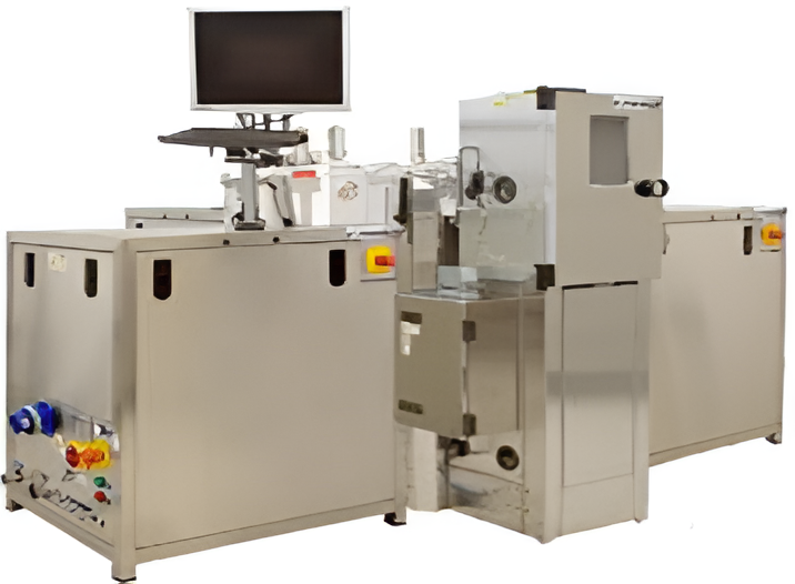
Memsstar
Advanced MEMS devices cannot be produced using conventional semiconductor manufacturing technology. The massive increase in MEMS applications requires the development of new process flows and integrated manufacturing techniques to quickly establish low cost, high quality advanced technology manufacturing. Dedicated to the development and advancement of MEMS specific processes, memsstar® offers process solutions for all MEMS release and surface modification applications. With our modular design our process modules can easily be extended from R&D through to volume manufacturing.
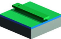
Release Processing
Isotropic etching removes sacrificial materials, and “releases” the 3D MEMS structure. The structure now has ‘free surfaces’ which are pristine and residue free. No pre-treatment, rinse or dry required, fast process times and wide process windows.
>> Release Etch >
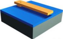
memsstar® SVRT™ process modules are used to remove all the sacrificial material quickly without leaving deposits or residues, and with undamaged surfaces
memsstar® offers the following SVR products
SVR – Xe
Based on XeF2 chemistries
SVR-VHF
Based on anhydrous HF chemistries
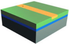
Surface Modification
Ultra thin films create very conformal coatings for MEMS. These are increasingly used in a wide variety of MEMS and nanodevices to deliver specific surface properties and lifetime reliability.
Surface modification and coating
The SPDT™ process module from memsstar® offers a wide range of standard film processes including moisture barriers, wetting layers, anti-stiction coatings, seed layers, bio-inert surfaces and many others. Traditional liquid immersion, or stagnant gas vapour phase systems can be limited by poor process control, slow process times, and coverage of aggressive feature shapes. memsstar® uses unique CCFFT™, and ultra thin films are quickly and repeatably deposited for optimised device properties.
Another unique capability is that this surface modification can be done immediately after the release etching process. memsstar® enables the MEMS surfaces to be treated whilst in pristine condition, which is as soon as they have been etched and without breaking process vacuum. This delivers superior film characteristics, in terms of durability and coverage.
memsstar® processes are the ideal solution for advanced etch and surface modification schemes with the integration of the SVRT™ and SPD™ process modules on a single platform.
All memsstar® processes are single wafer processes providing excellent repeatability wafer to wafer, large process windows for process optimisation, high yield and utmost control.
All process modules are available in 3 levels of automation and are upgradeable though the range.
- Solo platform: Standalone process module
- Sentry platform: Single wafer vacuum loadlock
- Multi platform: