TTL
Top Technology Limited, founded in 2005, develops, produces and globally distributes innovative and creative technologies for a variety of high-tech industries. Initially focused on plasma systems and processes for the semiconductor industry, the company’s plasma processing systems are now also used to manufacture LED lighting, solar cells, compound semicondutor, MEMs and opto-electronic devices and many other leading-edge products. With a focus on quality and customer-value enhancement, TTL continues to invest in process and equipment developments to meet the latest requirements of its customers.
Star+ series supports a range of customers involved in research, development and production with high performance and flexible tool configurations.
Star+ series platforms:
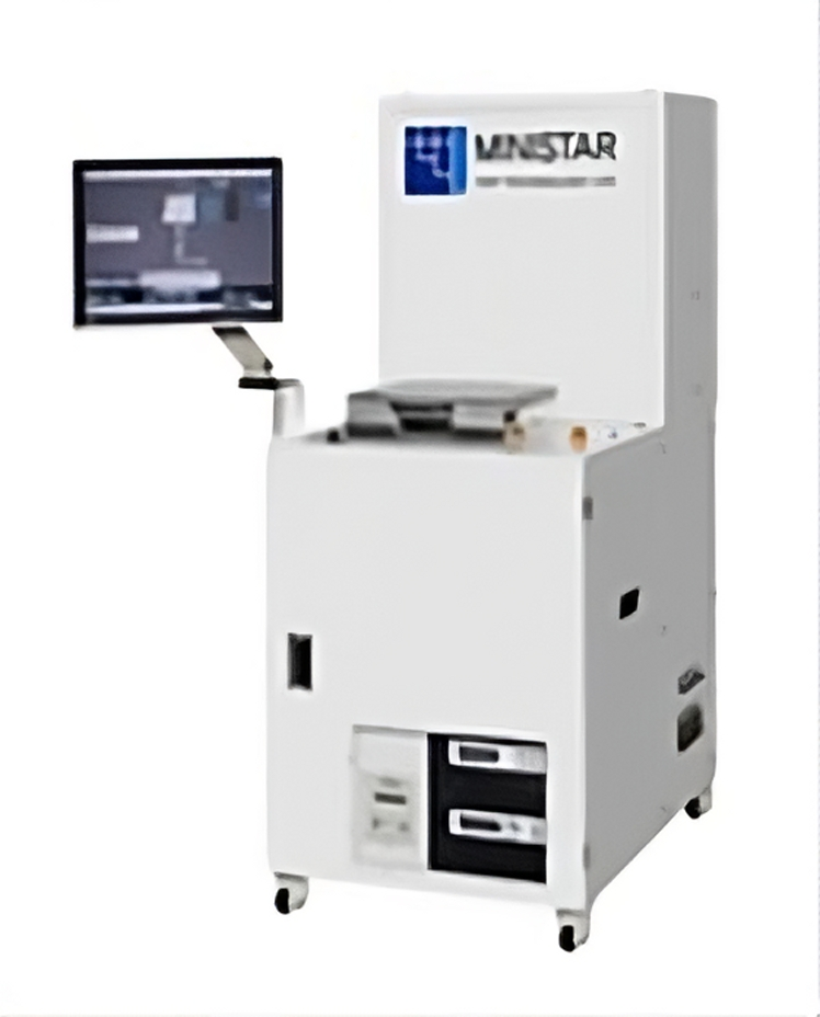
- MiniStar+, Open Load Etch & Deposition Tool up to 5 inch wafer
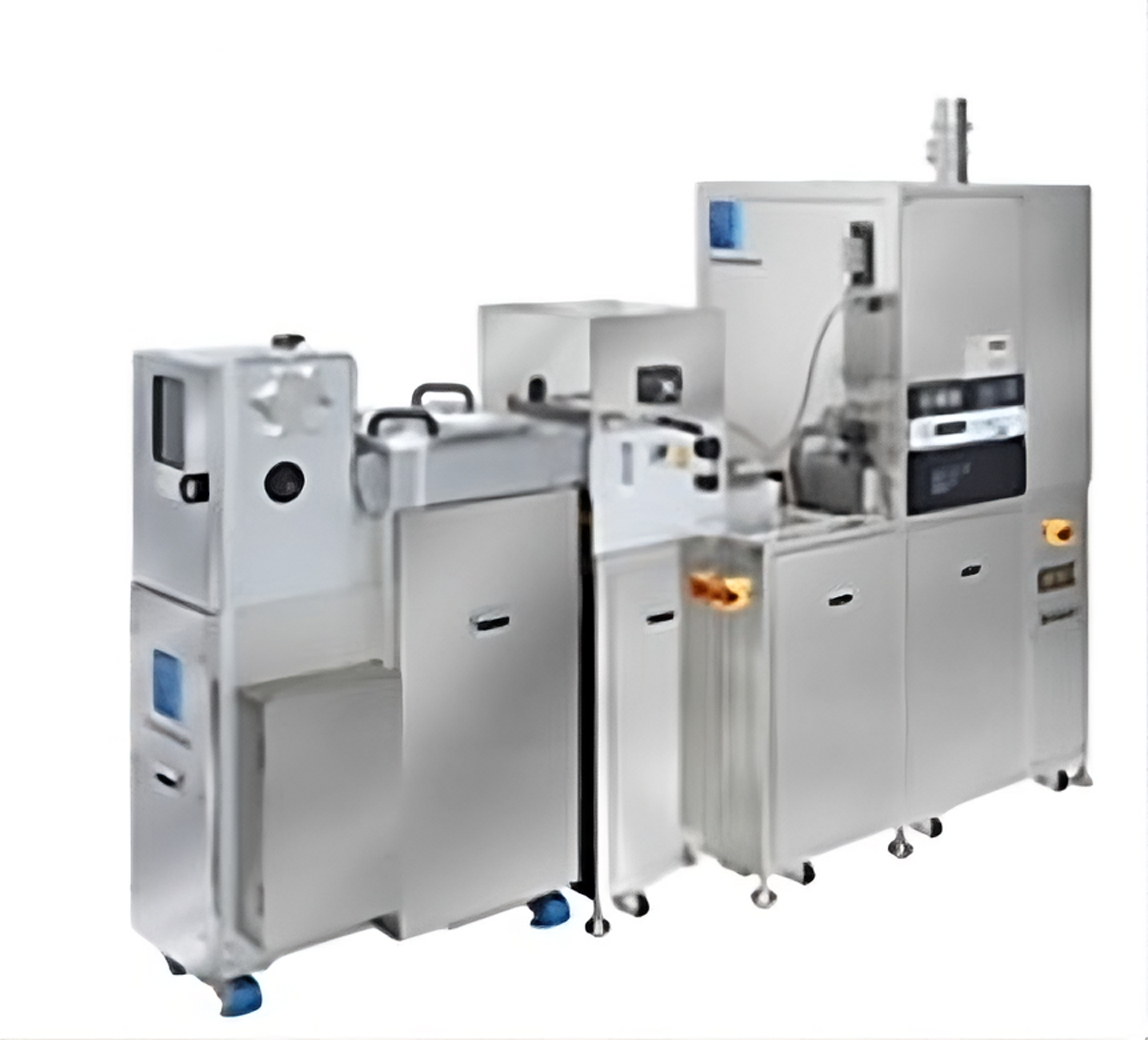
- LabStar+, Open Load Etch & Deposition Tool up to 12 inch wafer FabStar+, Load-locked Etch & Deposition Tool
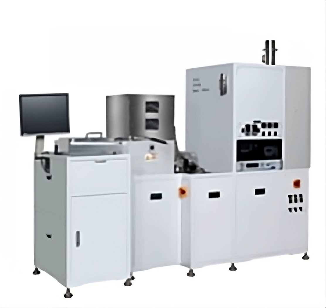
- CluStar+, Cassette to Cassette & Multi-chamber
- System up to 4 PMs and 2 VCE
Process chamber configurations:
- Inductively Coupled Plasma Etch (ICP)
- Inductively Coupled Plasma Chemical Vapor Deposition (HD-PECVD)
- Plasma Enhanced Chemical Vapor Deposition (PECVD)
- Reactive lon Etch (RIE)
Etch Application:
- Anisotropic etching of all types of silicon-based films for ULSI devices
- Etching of GaAs, GaN, InP and other compound semiconductor materials Low-damage etching of III-V compounds
- Fabrication of waveguide devices
- Etching of metal films-Cr, AI, W, Au, Pt and others
- Patterned sapphire etching for LED
- Polymer etch, photoresist strip and surface cleaning
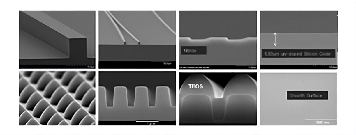
Deposition Application:
- High-rate and high-quality deposition of undoped and germanium-doped (for waveguide) silicon dioxide
- High quality silicon nitride deposition with stress control
- Amorphous silicon deposition
- Silicon oxynitride deposition
- Poly-silicon deposition
- Silicon carbide deposition
- Diamond like carbon deposition